His discoveries in the field of two-dimensional materials applied to electronic circuits have elevated him to the forefront of nanotechnology and artificial intelligence research, as reflected by the front covers of the most prestigious scientific journals in the field. Following these pioneering results, he was offered a position he couldn’t refuse at the King Abdullah University of Science and Technology (KAUST) in Saudi Arabia, a dream for any researcher due to the sheer volume of resources it provides.
This country is “a great unknown to Europeans,” says Lanza. “People’s think you’re crazy for coming here. There are a lot of outdated stereotypes, but countries in the Middle East are opening up quickly because they need to diversify their economies, so there are a lot of new job opportunities being created.” At this unique university, “thanks to its investment policies and Stanford-quality labs,” and along with half of his team from China, Lanza can focus on research and pursue his pioneering experiments. In fact, his latest finding is also revolutionary; he has developed an advanced encryption system using an electronic memristor circuit (rather than the usual transistor circuit) made from hexagonal boron nitride, a two-dimensional material with exceptional properties.
This work, published in the Advanced Materials journal in May 2021, allows numeric keys to be highly randomly generated for secure online payments, network connections or encrypted services in the context of the so-called Internet of Everything (IoE), i.e., the intelligent interconnection of people, processes, things and data. And it does all this while consuming very little energy, making it rather attractive for portable and self-powered (battery-free) technologies.
First step toward the future of electronics
In October 2020, Nature Electronics dedicated its cover to the research carried out by Lanza’s team, which is a pioneer in creating new hardware for implementing artificial intelligence. The team developed memristors made from hexagonal boron nitride, allowing them to emulate an artificial neural network for image recognition.
This means that the hardware of phones and other devices can be equipped with artificial intelligence more effectively than when using traditional memristors. The truly unique thing about this work is that they “obtained a yield of 98 percent, which is extraordinary in two-dimensional materials — no one has even come close to that number. Memristor circuits can be grouped three-dimensionally and you can fit a lot more in less space, and they’re also much cheaper to manufacture,” explains the engineer. Lanza and his team have paved the way for a new path that others are now researching, and have positioned themselves as cutting-edge trailblazers in the field of nanotechnology. They broke new ground, and they remain pioneers because it was them that invented it.
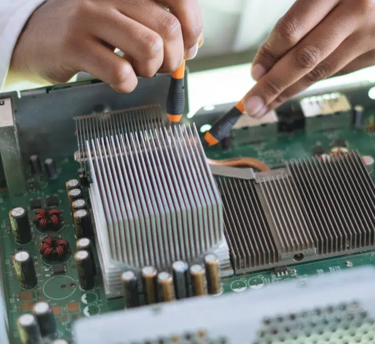
Lanza explains that three types of materials—conductors, semiconductors and insulators—are required to produce an electronic circuit. A lot of research has been done with two-dimensional conductive and semiconductive materials, but there has been considerably less activity when it comes to isolators — precisely the specialty of the Spanish researcher, whose experiments focus on hexagonal boron nitride, “the most insulating two-dimensional material.”
Another great achievement of the team spearheaded by Mario Lanza is its ability to use a peculiar tool (called an atomic force microscope with conductive tip), which allows the properties of insulators to be measured in a unique way, providing extremely accurate performance and variability data.
Phones, computers and devices unlike anything we’ve ever seen before
“Two-dimensional materials have far superior physical, chemical, electronic, mechanical, optical and magnetic properties than normal materials. For example, they have a high electrical conductivity, are very mechanically resistant, are practically transparent and conduct heat very well, which is an extremely important feature because whenever circuits and electronic devices fail, it’s always due to heat.” Memristors are used both for storing information, like a memory, and for processing it, just like artificial neural networks, logic gates and random number generators do.
Two-dimensional materials do not exist naturally, says the professor and, as such, a process must be carried out so that atoms adopt that arrangement. At present, synthesis processes are being performed to allow these materials to be manufactured industrially, and Europe is leading the way, he explains. “The semiconductor industry has begun to include these materials in its laboratory processes. It’s trying to make them compatible with the systems used to manufacture industrial circuits. When you have four industry-leading companies trying to integrate it into their own manufacturing processes, you can be quite certain that something is going to happen — that sooner or later this will become a commercial reality.”
The group’s findings will ultimately create devices that work better, i.e., that consume less power, are faster and lighter, and have a longer service life thanks to heat dissipation. What’s more, “they will make it possible to manufacture devices that do not yet exist. For example, producing circuits with flexible, transparent sensors or devices so that they can be fitted in the skin to monitor biomedical constants or in lenses for image processing.”
With regard to the future of artificial intelligence in the field of electronics, Lanza is clear that it will have an enormous impact on all learning tasks in image and sound recognition and, above all, for the IoE. In the field of materials, artificial intelligence is being used to optimize synthesis processes.
Two-dimensional materials to overcome stagnation
In the last 50 years, electronics have focused on making transistors smaller — so much so that “a physical limit has been reached; we’re at the point of reaching an atomic scale, so it cannot be reduced any more.” That’s why new materials (two-dimensional materials, which improve performance and the number of applications) and components such as memristors are now being researched. These two avenues of research are expected to lead to an increase in processing capacity and data storage. “It’s quite a challenge, but there’s no other option to overcome stagnation.”
The race to achieve this goal is extremely close among the three major companies (and countries) that manufacture transistors on a large scale: Taiwan’s TSMC, the world leader that has developed the smallest and most reliable transistors, closely followed by Samsung from Korea and the US firm Intel. “There’s an intense war. The Chinese also want to make their own chips, but that is the only thing they haven’t yet been able to replicate and it will cost them a lot.”
Spain is very well positioned in the field of two-dimensional materials, but much more could be done, says Lanza. “The scientists are highly qualified; the problem is resources. If researchers don’t have the resources, it’s very difficult to compete with those from other countries. And while it is also true that scarcity increases ingenuity, you can’t always work that way, you need more money from the government.”